Modern pluggable optics are hitting a physical power wall where the energy needed to push data across a circuit board costs more than the bandwidth provides. As artificial intelligence clusters grow toward 100 terabits per second for every node, the industry is moving toward co-packaged optics to stop the energy loss common in front-panel modules. By moving the light engine off the edge of the board and onto the processor itself, engineers can skip the limits of copper wires. This shift changes the very boundary between chips and light because the bottleneck has moved from the speed of the switch chip to the efficiency of the connection interfaces. Solving this requires moving away from separate parts toward fully combined light-based systems.
The Impending Physical Limits of Pluggable Optics
In standard data center switches, data moves from the main switch chip across a printed circuit board to reach a pluggable module at the front. As signal speeds move from 112G to 224G for every lane, the electrical signal fades and distorts over just a few centimeters of copper. To fix this signal loss, engineers must use complex chips called Retimers that eat a massive amount of power. The energy cost of driving these fast signals across the board strains the system for 1.6T modules and beyond. For a 51.2T switch, the power needed just to move bits to the front panel can take up 20% of the total energy. This creates a trade-off where faster speeds require so much cooling that it limits how many servers fit in a rack.
Pluggable modules like QSFP-DD are reaching their heat limits because 800G modules often give off 20 watts of heat each. When a technician packs 64 of these modules into one small chassis, the heat becomes nearly impossible to manage with fans. Moving toward 102.4T capacities would require modules that use even more power, making the front panel a wall that stops further growth. By shortening the electrical path, co-packaged optics can cut connection power use by half for every bit of data. Detailed testing shows that these setups can achieve a detailed breakdown of energy savings from APNIC, which helps maintain the global chip supply chain as demand for AI chips grows.
High-Frequency Signal Degradation and SerDes Limitations
The physics of high-speed copper traces create a natural ceiling for data transmission. When electrical pulses travel at high frequencies, they tend to move along the outer skin of the conductor, which increases resistance and generates heat. This phenomenon makes it difficult for the switch to maintain signal clarity without massive amplification. At 224G, the copper traces act like antennas, leaking energy and picking up noise from nearby lanes. Engineers currently use digital signal processors to clean these messy signals, but these processors generate their own heat and take up valuable space on the board. By bringing the optics closer to the logic, the system avoids these long copper paths entirely, allowing the switch to maintain a clean signal with much less effort.
The move to integrated light also changes how we think about reach. In traditional setups, the distance between the switch chip and the transceiver limits how fast the port can run. If the trace is too long, the signal dies before it reaches the fiber. Integrated systems remove this distance, placing the optical modulator within millimeters of the core logic. This proximity means the switch can use simpler drivers that don’t need the heavy lifting of modern retimers. This simplifies the board design and reduces the number of parts that could fail over time.
Technical Mechanics of Co-Packaged Optics Integration
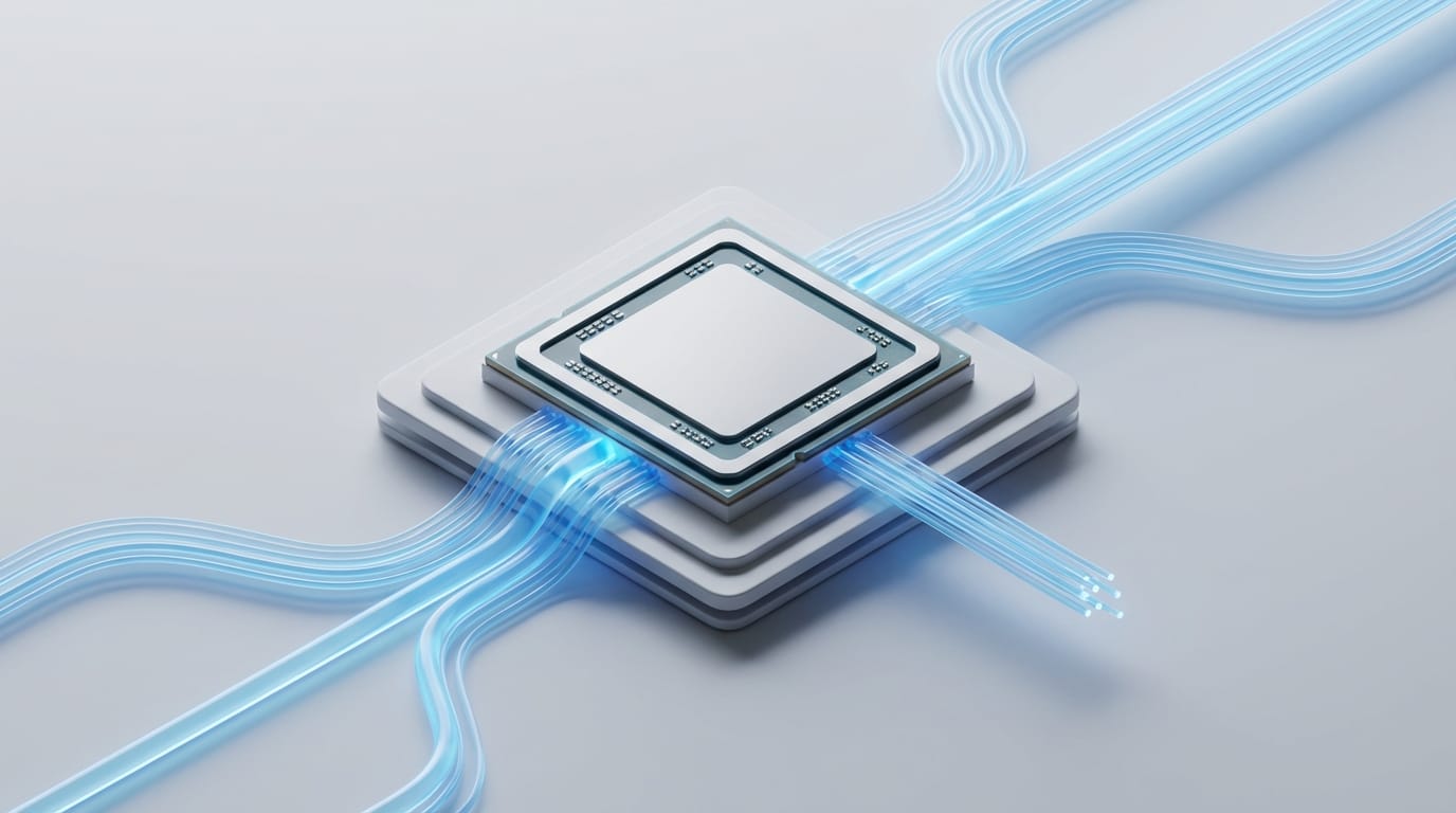
The main fix in co-packaged optics is how close the light engine sits to the switch chip. Instead of putting the optics on the front panel, the factory places the light engines on the same module as the main processor. This change cuts the electrical path from 20 centimeters to less than 10 millimeters, which lets the system use simpler and lower-power interfaces. This closeness allows the system to work as one unit instead of a group of separate parts. By removing high-power retimers, the entire signal path becomes more efficient because the main chip can drive the light engine directly. This marks a major change in how modern data centers function, moving away from parts at the edge toward parts at the core.
The Role of Silicon Photonics in 2.5D and 3D Packaging
Silicon photonics is the tech that lets light-based parts grow on standard silicon wafers. By putting lasers, modulators, and sensors onto a silicon chip, factories can use advanced stacking methods to save space. In a 2.5D setup, the main chip and the light engines sit side-by-side on a thin base; 3D stacking goes further by putting the optics right on top of the processor. This layout provides the density needed for next-generation networks. While a traditional front panel has limited space for plugs, this new method allows thousands of fibers to connect to the chip package directly. This skips the front panel bottleneck and enables switch speeds that would be impossible with standard plugs.
Modern manufacturing now relies on high-precision tools to align these fibers with the silicon waveguides. Because light waves are much smaller than electrical wires, even a tiny misalignment can cause the signal to drop. Factories use automated V-groove systems to lock the fibers into place, ensuring that light flows smoothly from the glass into the silicon. This level of precision was once only possible in labs, but it is now moving into high-volume production. As these processes get better, the cost of making integrated light systems will drop, making them more common in every data center.
The Reliability Paradox in Integrated Photonic Systems
While putting optics on the chip solves power problems, it creates a reliability puzzle. In a standard setup, if a plug breaks, a worker can just swap it for a new one without turning off the switch. In a combined environment, the optics are glued to a switch chip that can cost more than a luxury car. A small flaw in one laser could make the entire expensive chip useless. This creates a big risk for data center owners who need their systems to stay on all the time. If the light parts fail faster than the silicon parts, the whole system becomes less reliable. To solve this, the industry keeps the parts that fail most often separate from the main package.
External Laser Sources as a Serviceability Necessity
The most common fix for the reliability puzzle is using light sources that sit far away from the chip. Since lasers hate heat and are the parts most likely to break, moving them away from the hot switch chip helps them last longer. Organizations have created the official ELSFP specifications from the Optical Internetworking Forum to define a front-panel module that sends light to the internal engines through a fiber. By using this setup, workers can swap the laser source without touching the main switch chip. This keeps the laser cool and ensures the light source stays in a steady environment. This method keeps the power gains of co-packaged optics while keeping the ease of repair that engineers expect.
Using a remote laser also allows for better power management across the entire rack. A single large laser can sometimes provide light for multiple ports, which improves efficiency compared to having many small lasers running at once. It also means that the heat from the laser does not add to the heat of the processor, making the thermal design of the switch much simpler. This separation of duties is key to building systems that can run for years without needing a full hardware replacement. Further industry updates on the ELSFP standard show that more companies are agreeing on how these light modules should connect.
Performance Impacts on Next-Generation Fabric Design
As we move into the era of 51.2T networking, integrated light becomes a must. The number of fast lanes needed for these switches is almost impossible to wire on a standard board to a traditional front panel. New chips use co-packaging to hit full speeds while staying within a safe power range. This helps with managing data center power usage as AI tasks get heavier. Future switches will likely push this even further, needing even faster lanes. At these speeds, the signal requirements are so strict that the tiny paths of these integrated systems are the only way to keep the data clean. These designs will lead to flatter networks with fewer steps between servers, which lowers delay for AI training jobs.
The shift to these architectures also changes how we think about network latency. In a traditional network, every time a signal moves from a chip to a copper trace and then to an optical module, it picks up a small amount of delay. While each delay is tiny, they add up across thousands of nodes in a large cluster. Integrated light reduces the number of transitions the signal must make, which helps AI models synchronize faster. This speed is vital for large language models that need to share massive amounts of data across hundreds of GPUs every second.
Thermal Management Shifts from Air to Advanced Cooling
Putting so much power in one spot shifts the cooling job from the front panel to the center of the board. Because the main chip and the light engines are now one piece, they get hotter than fans can handle. This is pushing the industry toward liquid cooling where cold plates sit directly on the chips. Liquid cooling removes heat much better than air, keeping both the silicon and the light parts at the right temperature. While this makes the rack design more complex, it is a necessary trade for hitting the high speeds needed by modern AI. The growth of cooling tech is now just as important as the growth of the chips themselves.
Liquid cooling also allows for much denser hardware designs. Without the need for large air channels and bulky heat sinks, engineers can pack more switching power into a single rack unit. This density is a primary goal for cloud providers who want to maximize the performance of their existing real estate. While the initial cost of plumbing a data center for liquid is high, the long-term energy savings and performance gains usually justify the investment. We are seeing a transition where the cooling system is no longer an afterthought but a core part of the architectural plan.
Standardization and the Path to Commercial Adoption
For these new systems to work everywhere, the industry must avoid being locked into one brand. Group efforts ensure that light engines from one maker work with switch chips from another. This includes building the laser standards that provide a common way for modules to connect. This teamwork is vital because large companies rarely buy all their gear from one place. Making sure the way light moves to the package is standardized allows for a healthy market. Without these rules, the high cost and complexity of integrated light would limit its use to only the most specialized AI labs.
Moving to this new method also changes the cost of making chips. Factories must now manage good dies for both logic and light at the same time. Testing these modules is much harder than testing a standard chip because it involves checking both electricity and light at the same time. If the light parts fail during testing, the whole expensive package might be thrown away, which raises costs. This is why manufacturing skill is the final hurdle. As factory processes for light chips get better, the cost for every bit will drop below the cost of old plugs, making integrated light the standard for the future.
The move to co-packaged optics shows that we can no longer treat the network and the processor as separate things. As the energy cost of moving data starts to equal the cost of processing it, the physical gap between silicon and light must shrink. This integration fixes the power wall but needs a new plan for reliability through remote lasers and liquid cooling. The success of this tech will be measured by how well it makes the network invisible, letting AI grow without being held back by the physics of copper wires. Designing the next generation of data centers will require a careful balance between extreme density and the need for easy repairs in the field.